India का ₹1.27 Lakh Crore Semiconductor Mission 2.0: क्या अब India सिर्फ Chip Assembly नहीं, पूरी Semiconductor Supply Chain बनाएगा?
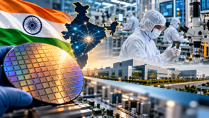
Keywords: Semiconductor India, India Semiconductor Mission 2.0, Chip Manufacturing India, Chip Design India, Semiconductor Industry
Semiconductors आज सिर्फ smartphones या computers के components नहीं हैं। AI servers, electric vehicles, telecom networks, defence systems, satellites, automobiles और data centres—लगभग हर modern technology की foundation semiconductor chips पर टिकी है। यही वजह है कि India अब semiconductor race में सिर्फ manufacturing capacity बनाने के बजाय पूरी value chain पर पकड़ मजबूत करने की कोशिश कर रहा है।
इसी strategy को आगे बढ़ाने के लिए Union Cabinet ने 15 July 2026 को Semicon 2.0 को ₹1,27,500 crore के total outlay के साथ approve किया। इसका objective India को सिर्फ chip assembly या packaging destination बनाने के बजाय design, fabrication, advanced packaging, equipment, materials, R&D और skilled talent वाला complete semiconductor ecosystem बनाना है।
Semicon 1.0 से Semicon 2.0 तक क्या बदला?
India Semiconductor Mission का पहला phase मुख्य रूप से semiconductor manufacturing ecosystem की foundation तैयार करने पर focused था। Government ने fabs, ATMP/OSAT facilities और Indian-designed chips को support करने के लिए Semicon India Programme शुरू किया था।
अब दूसरा phase कहीं ज्यादा broad है।
Government के अनुसार Semicon 2.0 के छह strategic pillars हैं:
- Chip Design
- Semiconductor Equipment & Materials
- More Fabrication Facilities
- Advanced Packaging / ATMP
- Research & Development
- Talent Development
यानी strategy अब सिर्फ “India में chip बनाओ” तक सीमित नहीं है। Focus यह है कि chip बनाने के लिए जरूरी technology, machines, materials, design capability और skilled engineers भी India में develop हों।
India में Semiconductor Manufacturing कितनी आगे बढ़ चुकी है?
यह mission अभी केवल announcements तक सीमित नहीं है।
Government के latest data के मुताबिक Semicon India Programme के तहत 12 semiconductor projects को छह states में approval मिल चुका है, जिनकी committed investment ₹1.64 lakh crore से ज्यादा है। इन projects में silicon और compound semiconductor fabs, display fabrication और advanced packaging facilities शामिल हैं।
September 2026 तक पांच semiconductor units commercial production शुरू कर चुकी थीं, जो यह संकेत देता है कि India semiconductor policy से actual manufacturing phase में प्रवेश कर रहा है।
यह बदलाव महत्वपूर्ण है, क्योंकि semiconductor industry में credibility सिर्फ investment announcements से नहीं बल्कि actual production, yield, quality और global customer acceptance से बनती है।
सबसे बड़ा बदलाव: Chip Design पर Focus
India की semiconductor story का एक बड़ा advantage पहले से मौजूद है—engineering और chip-design talent।
Government के अनुसार India में लगभग 20% global semiconductor chip-design workforce मौजूद है और country में semiconductor domain से जुड़े Global Capability Centres भी significant scale पर हैं। Semicon 2.0 इस existing strength को product और intellectual-property creation में बदलने की कोशिश कर रहा है।
Latest implementation update के अनुसार government अब 200 chip-design companies का ecosystem build करने का target रख रही है। करीब 400 engineering colleges और 105 startups को industry-grade Electronic Design Automation यानी EDA tools तक access देने की दिशा में भी काम हो रहा है।
इसका long-term impact काफी बड़ा हो सकता है।
अगर India केवल foreign companies के लिए chip designs develop करने के बजाय अपने architecture, IP और application-specific chips create करता है, तो value addition manufacturing से कहीं ज्यादा बढ़ सकती है।
Fab जरूरी है, लेकिन Fab अकेला काफी नहीं
एक semiconductor fab बेहद complex infrastructure होता है। इसमें clean rooms, advanced machinery, chemicals, gases, water treatment, power infrastructure और highly specialised workforce की जरूरत होती है।
लेकिन chip manufacturing की supply chain fab के बाहर भी बहुत बड़ी होती है।
यहीं Semicon 2.0 का materials और equipment focus महत्वपूर्ण हो जाता है।
Semiconductor manufacturing में high-purity gases, specialty chemicals, wafers, manufacturing equipment और precision components की आवश्यकता होती है। अगर इन inputs के लिए India को लगातार imports पर निर्भर रहना पड़े, तो domestic semiconductor ecosystem की resilience सीमित रहेगी।
इसलिए Semicon 2.0 का objective raw materials से लेकर finished chips तक broader domestic ecosystem develop करना है।
Advanced Packaging क्यों बन रहा है अगला बड़ा Opportunity?
Semiconductor industry में chip बनाना ही अंतिम step नहीं है।
ATMP यानी Assembly, Testing, Marking and Packaging और OSAT यानी Outsourced Semiconductor Assembly and Test facilities chips को final usable components में बदलने में critical role निभाती हैं।
Advanced packaging की importance AI और high-performance computing के बढ़ने के साथ और ज्यादा बढ़ रही है, क्योंकि modern chips में performance, power efficiency और thermal management के लिए packaging technology increasingly important हो रही है।
India ने Semicon 1.0 में packaging ecosystem की foundation रखी थी। Semicon 2.0 अब इसे advanced packaging capabilities तक ले जाने की कोशिश कर रहा है।
India के लिए यह सिर्फ Technology Mission नहीं है
Semiconductor ecosystem का impact electronics sector से कहीं आगे जा सकता है।
अगर domestic supply chain मजबूत होती है, तो इसका फायदा:
Automobiles → EVs → Smartphones → Telecom → Defence → Aerospace → AI Data Centres → Consumer Electronics
जैसे sectors को मिल सकता है।
Government का broader objective domestic value addition बढ़ाने के साथ supply-chain resilience और technological self-reliance को strengthen करना है।
Global semiconductor supply chains में geopolitical tensions और disruptions ने भी countries को domestic manufacturing capabilities पर ज्यादा ध्यान देने के लिए मजबूर किया है।
ऐसे environment में India के लिए semiconductor capability सिर्फ economic opportunity नहीं, बल्कि strategic capability भी बनती जा रही है।
लेकिन ₹1.27 Lakh Crore का मतलब क्या है?
यहां एक important distinction समझना जरूरी है।
₹1,27,500 crore Semicon 2.0 का government-approved programme outlay है। इसे सीधे semiconductor companies द्वारा किए जाने वाले total investment के बराबर नहीं समझना चाहिए।
इसके अलावा Semicon India Programme के तहत पहले से approved projects की committed investment ₹1.64 lakh crore से ज्यादा बताई गई है। इसलिए government support, private investment और project commitments को अलग-अलग numbers के रूप में देखना जरूरी है।
यानी actual semiconductor ecosystem में आने वाली total economic activity केवल ₹1.27 lakh crore तक सीमित नहीं होगी।
सबसे बड़ी चुनौती: Scale और Execution
Semiconductor industry में पैसा लगाना पहला step है। असली challenge है yield, technology, reliability और scale।
एक fab successfully build करना और globally competitive semiconductor manufacturing operation चलाना दो अलग बातें हैं।
India को आने वाले वर्षों में कई challenges solve करने होंगे:
- Highly skilled semiconductor engineers की availability
- Advanced manufacturing equipment
- Reliable power और water infrastructure
- Semiconductor-grade materials
- Global customers और supply contracts
- Technology transfer और R&D
- Manufacturing yield और quality
- Long-term private investment
- Global semiconductor companies के साथ deeper partnerships
इसीलिए Semicon 2.0 में talent और R&D को अलग pillars के रूप में रखा गया है। Government के अनुसार पिछले चार वर्षों में लगभग 70,000 design engineers को train किया गया है, जबकि future focus system design और precision manufacturing तक capabilities expand करने पर है।
क्या India Taiwan या South Korea को compete कर सकता है?
Short answer है—immediately नहीं।
Taiwan, South Korea, Japan और US ने semiconductor ecosystem को decades में build किया है। Advanced semiconductor manufacturing में technology, capital, intellectual property और supply-chain relationships की complexity बहुत ज्यादा है।
लेकिन India को शुरुआत से हर segment में compete करने की जरूरत भी नहीं है।
India की strongest entry points हो सकते हैं:
Chip Design + Embedded Systems + Compound Semiconductors + Advanced Packaging + Semiconductor Services + Equipment/Materials + Talent
यानी India अपनी existing engineering strength को manufacturing ecosystem के साथ जोड़कर gradually higher-value semiconductor chain में move कर सकता है।
India की Semiconductor Story का अगला Phase
Semicon 1.0 ने सवाल का पहला हिस्सा address किया—“क्या India में semiconductor manufacturing हो सकती है?”
अब Semicon 2.0 का बड़ा सवाल है:
“क्या India semiconductor की पूरी value chain में globally relevant बन सकता है?”
अगर design companies, fabs, advanced packaging units, equipment suppliers, material manufacturers, R&D centres और skilled workforce एक-दूसरे के साथ scale कर पाते हैं, तो India सिर्फ chips assemble करने वाला market नहीं रहेगा।
वह semiconductor ecosystem का design, manufacturing और innovation hub बनने की दिशा में आगे बढ़ सकता है।
₹1.27 lakh crore का mission इसलिए सिर्फ एक government scheme नहीं है। यह India की technology economy को low-to-mid value electronics manufacturing से high-value semiconductor ecosystem की तरफ ले जाने की long-term bet है।
अगले कुछ वर्षों में असली test announcements का नहीं, बल्कि commercial production, Indian chip IP, global customers और supply-chain depth का होगा।
अगर यह execution सफल रहा, तो “Made in India” electronics के साथ अगला बड़ा सवाल शायद यह होगा—
“Designed in India, Made in India — और Powered by Indian Semiconductor Technology?”